

University of Wisconsin-Madison engineers and physicists have developed a method of measuring how strain affects thin films of silicon that could lay the foundation for faster flexible electronics.
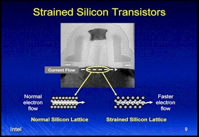
Silicon is the industry standard semiconductor for electronic devices and silicon thin films have the potential to produce faster, more flexible electronics. Researchers have long known that inducing strain into the silicon increases device speed, yet have not fully understood why.
Developed by a team of researchers led by Max Lagally, the Erwin W. Mueller and Bascom Professor of Materials Science and Engineering at UW-Madison, the new method enables the researchers to directly measure the effects of strain on the electronic structure of silicon. The group published its findings in the Oct. 10 online edition of Physical Review Letters, and the paper will soon appear in the journal's print edition.
Standard strained silicon has so many dislocations and defects that strain measurements are inaccurate, so the research team starts with its own specially fabricated silicon nanomembranes. The team can induce uniform strain in these extremely thin, flexible silicon sheets.
"Imagine if you were to attach a ring and a hook on all four corners and pull equally on all four corners like a trampoline - it stretches out like that," says Lagally.
As a result, the researchers avoid the defects and variations that make it difficult to study standard strained silicon. Uniform strain allows accurate measurement of its effect on electronic properties.
The researchers drew on the powerful X-ray source at the UW-Madison Synchrotron Radiation Center (SRC), which allowed them to measure conduction bands in strained silicon. To study the energy levels, the researchers needed a wavelength-tunable X-ray source. The SRC also houses a monochromator, a device that enabled the team to choose a precise wavelength, giving their readings the required high energy resolution.
By measuring nanomembranes with different percentages of strain, the researchers have determined the direction and magnitude of shifts in the conduction bands. Their findings have shed light on divergent theories and uncovered some surprising properties. Understanding these properties, and the energy shifts in strained materials, could lead to the improvement of fast, flexible electronic devices.
Capitalizing on its techniques for fabricating silicon nanomembranes, the group hopes to use SRC resources to study strain in other semiconductor materials, as well as to make measurements over smaller areas to study the effects of localized strain.
"The ability to make membranes of various materials, to strain them, and make these measurements will enable us to determine strain-dependent band structure of all kinds of semiconductor materials," says Lagally.
Companies using strained silicon techniques
Chip firms are always looking to gain an edge over their competitors in a market worth over $100 billion a year and the one silicon strategy for faster chips that has proven to be cost effective in mass production is - strained silicon.
In 2001 IBM strained silicon to boost chip speeds up to 35 percent and another strained-silicon technique used to create faster chips was adopted by Intel in 2002. Advanced Micro Devices incorporated strained silicon into all their 90-nanometer chips in 2004.
Global semiconductor foundry, UMC, Taiwan, announced last month that it has manufactured the foundry industry's first fully functional 28nm SRAM chips. The chips are based on UMC's independently developed low-leakage (LL) process technology. UMC utilized advanced double-patterning immersion lithography and strained silicon technology to produce the chips, which feature very small six-transistor SRAM cell sizes of approximately 0.122 um2.
The International Technology Roadmap for Semiconductors
The International Technology Roadmap for Semiconductors, known throughout the world as the ITRS, is the fifteen-year assessment of the semiconductor industry's future technology requirements. These future needs drive present-day strategies for world-wide research and development among manufacturers' research facilities, universities, and national labs.
The objective of the ITRS is to ensure cost-effective advancements in the performance of the integrated circuit and the products that employ such devices, thereby continuing the health and success of this industry.
The Roadmap teams identify critical challenges, encourage innovative solutions, and welcome participation from the semiconductor community. These teams are joining with other strategic roadmapping efforts (such as electronics and nanotechnologies) so the Roadmap effort comprehends the spectrum of needs for basic research capabilities and product potentials.
In a recent report "International Technology Roadmap for Semiconductors 2007 Edition," they state:
"In the starting wafer area, it is expected that alternatives to bulk silicon such as silicon-on-insulator substrates will proliferate. Additionally, various forms of strained silicon technology may be incorporated although these have been and continue to be principally achieved through value-added modifications to the integrated circuits manufacturing process.
Also, an important difficult challenge expected to emerge within the Roadmap horizon is the potential need for the next generation 450 mm silicon substrate. Based upon historical diameter change cycles, the industry is already several years behind the pace necessary to allow the next generation 450mm silicon substrate to be ready for device manufacture in the year 2012."
Reference: University of Wisconsin-Madison
For more attend Printed Electronics USA 2008 and Printed Electronics Europe 2009.
