The IDTechEx conference Printed Electronics Asia in Tokyo last week revealed several new trends in printed electronics. It is not yet certain whether printed organic photovoltaics and transistors represent the lowest cost routes to these devices. Because they are large in area, high yield is more difficult to obtain and more material is used. Organic materials are currently very expensive. However, they usually retain many useful features such as being safe for children to chew and being tightly rollable and shock proof. Copper indium gallium diselenide photovoltaics may dominate the flexible PV scene within ten years because of a good compromise of cost, environmental credentials, lightweight and rollability and more companies are entering this business.
Many reasons for smaller feature size
Where small feature size for large transistor counts plus high yield, high reliability and long life are important, nanosilicon and single layer Nano ePrint transistors, with over 1000 transistors per square millimeter, have an important place. In addition, more and more companies are backing transparent and potentially low cost metal oxide transistors, now printable using precursors. That usually involves indium zinc oxide. It is even increasingly common for companies to develop both metal oxide transistors for transparency and organic transistors for rollability, both being a route to lowest cost, it is now felt. For high mobility and therefore highest frequency of operation, inorganic printed transistors are increasingly attractive.
Betting on both horses
Examples of companies "betting on many horses" are Toppan Printing and Samsung. Indeed, Toppan Printing now backs nanosilicon, organic and zinc oxide transistors. Indeed, in materials supply, there is also a trend for corporations to increase their chances of creating a ten billion dollar business in printed electronics by developing inorganic, organic and composite formulations. For example, Kodak, Merck Chemical, Solvay, Agfa and Bayer have an increasingly broad repertoire. Feeding them are universities such as Cambridge University in the UK and the University of Tokyo with a similarly broad approach.
Transparent printed AMOLED display using printed InZnO transistors

Source: Samsung
Flexible, non-volatile, printed memory by Thin Film Electronics

Source: ThinFilm Electronics
Conference highlights on Day 2
Here are some highlights from the first stream of day 2 of the conference. Liquavista now has strong backing for what is considered its Second Generation LCD, consisting of flexible color video speed displays suitable for second-generation e-readers and other applications. It was claimed that any substrate could be used and it was argued that this flexible, robust technology would be used on mobile phones where, currently, 30% of returns are screen related. UK government funding of nearly $20 million has been obtained to get these displays into Plastic Logic e-readers.
Stretchable electronics
There are now many routes to stretchable electronics emerging, some with up to 400% extension. Single wall carbon nanotubes, polymeric elastomers and mesh or serpentine patterning are among these. Uses will be in healthcare, toys etc. In addition, the University of Cambridge in the UK and Tokyo University are working in this area. The latter even showed a video of stretchable electronics placed over an egg without breaking it.
Mixed printing technologies increasingly used
Mixed printing technologies in a single device are increasingly encountered, including combinations of micro-gravure, screen and ink jet. Operating voltages are coming down as demanded by the marketplace. For example, toys must not exceed 30 volts in many countries. Consider the 24 volt printed organic ferroelectric memory of Thin Film Electronics AB of Sweden, which collaborates with InkTec of Korea to achieve an impressive 95% yield reel to reel. It also collaborates with organic transistor printer PolyIC in Germany and others, applications now being envisaged as including toys and internet interactive gaming cards. Here electrodes are currently screen-printed but the ferroelectric memory polymer is printed by microgravure. Across the whole scene, however, ink jet is most commonly encountered because it wastes little ink and works well on uneven surfaces though throughput and wide area capability with ink jet is not the best.
Thin film technologies that are not yet printed are also encountered because they lead to higher performance devices and other advantages. On the other hand, the H.C.Starck self-assembling PEDOT-PSS monolayers of organic semiconductor attracted interest. In addition, many more people are chasing carbon nanotubes and graphene these days.
Progress with OLEDs
Kodak gave a masterly presentation on latest OLED materials, as one would expect from one of the three companies holding the majority of the key patents on the subject. Scalable white OLED for large TV was the topic - the speaker being Takatoshi Tsujimura, Senior Director, OLED Product Development, Kodak Japan Ltd. He covered "Scalable" Mura compensation technology; Global Mura Compensation - "Scalable" TFT technology including polysilicon and metal oxide transistors and the older silicon options; Scalable OLED technology; White+Color Filter; Synergy with OLED lighting; Technology proof for medium to larger AMOLED display and Scalable 100% NTSC 8.1"AMOLED display meeting with product specs.
His conclusions were :
Defect density strategy is very important when large AMOLED is
manufactured.
Combination of matured technology with Scalability should be the best for large area AMOLED TV.
Simple pixel circuit for repair strategy
GMC(Global Mura Compensation)
White +Color Filter OLED device
Scalable TFT Backplane method
White + Color Filter method has synergy with OLED lighting, as common infrastructure can be used.
A technology proof with White AMOLED Technology
Scalable 8.1" AMOLED with product-level performance
Medium-Large AMOLED can be made by combination of low risk technologies. = High yield, Fast ramp up.
Large AMOLED TV will be coming with low risk technology!
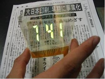
The picture below shows a transparent flexible OLED by Dai Nippon Printing, which presented at the conference.

Printing copper and other new inks
Printing copper to escape the volatility of the silver price is receiving increasing attention with Novacentrix and Applied Nanotech Holdings in the US offering formulations that escape the challenge of the insulating oxide usually created on copper. Several academic institutions are also working on printed copper, sometimes in nano form or using precursors. At the conference, Hitachi Chemical was a focus of attention when it announced its ink jettable copper ink that does not need a special environment. It is dispersant free because electrostatic repulsion of the nano particles of 10-100nm is employed. Remarkably, the resistivity of the resultant golden copper film is 6 ohm cm, near to bulk copper at 1.7 ohm cm. The dry curing process can be under 200C and sometimes under 100C.
Hitachi Chemical also announced organic insulating inks, an ink jettable resistor ink and a printable organic gate dielectric for transistors with permittivity of 3.5. Progress is rapid in this company. It even announced various substrates for printed electronics based on polyimide, cycloolyfins and acrylics.
RFID
Mighty Card gave an RFID tutorial to enable the audience to fully understand the subsequent lecture, which was by Professor Cho of Sunchon University Korea on his remarkable success in printing complete RFID tags using regular printing equipment. In line with the new trend, these employ inorganic semiconductors and dielectrics, ZnO based SC and barium titanate PMMA combination for the gate dielectric. Organic passivation is used in another example of increasingly common mixed chemistries. Carbon nanotubes have also been studied, so far with a modest 1 cm2/vs mobility but this increases to 9.5 cm2/vs at high current. Single bit tags are being followed with 16 bit tags, all at the world's most popular RFID frequency 13.56MHz. Paper substrates are of interest to reduce cost even further.
For more attend Printed Electronics USA 2009.


