

Conductive inks are a simple and unglamorous layer but they will constitute a hefty $2.86 billion market in 2012. As forecast by IDTechEx, in our new report Conductive Ink Markets 2012-2018, the market will rise to $3.36 billion in 2018, with $735 million captured by new silver and copper nanostructure inks.
The figure below shows our forecast and outlines the market segments covered in our analysis.
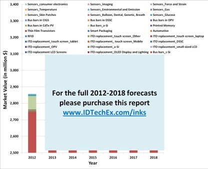
Forecasts covering 30 market segments
Source: IDTechEx www.IDTechEx.com/inks
These values make conductive inks the most successful segment of all printed electronics, surpassing the likes of printable OLEDs, photovoltaics, displays, etc. This is because conductive inks find use in a great variety of end applications, including RFID, photovoltaics, sensors, vehicles, smart packages, flexible displays and lighting and touch screens. This enormous diversity reflects the simple fact that electronic devices require multiple layers of interconnects.
This multiplicity of market requirements has resulted in the introduction of many types of inks, each offering their own set of characteristics and uniques, and therefore targeting different market segments. Innovation in the field of nanotechnology has largely enabled this high level of product differentiation. Indeed, the market today contains graphene, carbon nanotubes, and silver and copper nanostructure (nanoparticle and nanowire) inks, all of which have one or two dimensions in the nanoscale.
The table below compares overall attributes of several inks types and indicates possible target markets. Here, we have included only the silver- and copper-based products. The report itself however also covers silver-coated copper, graphene, carbon nanotubes, and PDOT:PSS.

A comparison of several conductive inks
Source: IDTechEx www.IDTechEx.com/inks
ITO replacement is a crowded market
Indium Tin Oxide (ITO) replacement is a broad and varied market, including touch screens, LCD screens, OLEDs, thin film photovoltaics, etc. ITO is typically sputtered onto a substrate and then patterned (if required) using a subtractive process. ITO gives excellent opto-electronic characteristics when processed on rigid substrates with annealing temperatures in excess of 250C. It can achieve 10ohm/sqr with an optical transmission of >85%. The performance is lower when ITO is deposited on a flexible (e.g., PET) substrate, which limits the maximum annealing temperature.
There has been a global push to replace ITO. This was driven by concerns over its cost and its long-term supply security. The latter concern was aggravated when the price of indium spiked five folds between 2004 and 2006 (i.e., in 2004 indium was sold at 200$/Kg while in 2006 it was at 1,000 $/Kg). the price concerns have largely eased since then as manufacturers stepped up productions and supply exceeded demand (in fact, the Chinese government had to intervene in 2008/9 to stop further price falls). This has shifted the competitive landscape for many alternative materials by pushing down the required market entry price points. Indeed, materials that looked cost competitive in 2006, now suddenly look overpriced again.
ITO does not withstand repeated bending or rolling. It can crack and its resistance increases by several orders of magnitude. This can be a handicap when considering flexible and/or rollable applications, which are therefore the best opportunity for ITO alternatives. Here however, ITO is often not the main factor limiting the realisation of flexible devices, but it is other factors such as barrier films, the lack of a clear market pull, thin film transistor backplanes, etc. Indeed, many target markets are still several years away.
We anticipate that ITO will remain the dominant transparent electrode. The device manufacturers have a diverse set of high-volume suppliers. They also have in-house facilities to recover the ITO that is wasted during the fabrication process. The capex is also largely depreciated. They will be reluctant to move away from ITO unless the replacement material can demonstrate secure high-volume supplies and a clear cost advantage.
Silver flakes will continue to reign supreme
Screen printable silver flake conductive inks command the largest market share of all printed conductive inks. The biggest markets are crystalline silicon photovoltaics (e.g., consumes >1,000 tonnes per annum) and switching membranes. Silver flake inks are a mature technology, offering very competitive prices and performance levels that are sufficient for most market needs. They will therefore be very difficult to displace.
Several developments in progress today may however open the space for other conductive inks. One example is the move towards ultra-thin crystalline silicon photovoltaics in order to slash costs (i.e., reduce the $/W metric). In turn, this may require the use of inkjet printing techniques to deposit the bus bars since the wafers may become too fragile for screen printing methods. Therefore, barring rapid improvements in screen printing technology, this change opens the door for nanoparticle-based inks because flakes are too big for inkjet printer nozzles. In fact, the need to print on fragile and/or irregularly-shaped objects will create market opportunities for nanoparticle inks.
Nanostructure inks will also find use in a range of emerging applications, including vehicle interior design, smart packaging, etc. Often these markets are characterised by the need for a technology push to create a market need, therefore suppliers are likely to have to move up the value chain and offer something more than an ink or a component, i.e., need products.
Nanostructure inks will become more cost competitive with silver flakes (on a cost per unit conductance method) in the mid term when scale up takes place and manufacturing costs are pushed down. Currently however, many suppliers are facing the classic chicken and egg problem i.e., to scale up and push the market or to wait for the market pull before sinking investment. The winners will be ones who establish strategic partnerships for scale-up today.
Report Overview
For a full analysis and 6 year forecasts by application, read Conductive Ink Markets 2012-2018. This report provides an in-depth review of printable conductive inks. For each ink, IDTechEx covers the underlying technology including an overview of the fabrication process; assesses their strengths and weaknesses; identifies and analyzes key technology and market drivers; and provides guidelines for price development in the future.
We assess and forecast the markets requiring silver and copper inks. We take a very granular approach in our assessment, looking into each sub-market in great depth and building our forecasting bottom up. The markets covered include crystalline and thin film photovoltaics, RFID, logic and memory, touch screens, displays, vehicles, consumer electronics, sensors and smart packaging.
Moreover, in each market segment, we forecast the market share by ink technology using our assessment of technology drivers, end-user requirements, and estimated price points. This enables us to forecast the value captured by each ink technology in each application.
To learn more, read Conductive Ink Markets 2012-2018.
For more information attend Printed Electronics Asia in Tokyo, Japan on October 2-3 - the key event to learn and network with the leaders in printed electronics in Asia. See Printed Electronics Asia, October 2-3, 2012 to register early for the best savings.
