The following highlights some of the major announcements from a recent printed electronics event.
Asahi Kasei - sub micron printing resolution
Japan-based Asahi Kasei has more than 25,000 employees around the World, operating in electronics, healthcare, chemicals and fibres. Researchers at the company have developed a roll to roll (R2R) high resolution printing method, demonstrating sub micron line resolution. The key enabling elements of this are the fabrication of a super smooth surface roller. This is coated, and then patterned using EBM. The roller has a 100mm diameter and width of 70mm (patterned width is 50mm). Using this, Asahi Kasei have printed super high resolution lines to 250nm. The company is working on other issues now such as registration of multiple layers at that resolution level.
Therasolve skin patch
Since Estee Lauder pulled the powered skin patch due to printed battery supplier going bankrupt, BioBliss took its place with a powered cosmetic patch. Another company to enter now includes Therasolve, this time targeting medication compliance in the form of a patch, called Memopatch, which is a skin patch which reminds the user when they need to take medication. The small flexible dermal patch gives its wearer a discreet 'digital touch' reminder stimulus when it is time to take a medication dose Further details of the product is due to be launched in the next few months.
Touch screen makers demand higher resolution
A significant growth area for conductive ink is in printing the conductive elements around the transparent conductive film, hidden under the bezels. The IDTechEx report Transparent Conductive Films gives a detailed breakdown of this opportunity, as highlighted below. However, as phones become smaller, so too is the need for smaller bezels i.e. higher resolution edge conductors. The industry is moving to 50 microns resolution, but 30 microns is their target.
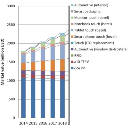
Market Size for Conductive Ink by Application Type. Source: IDTechEx
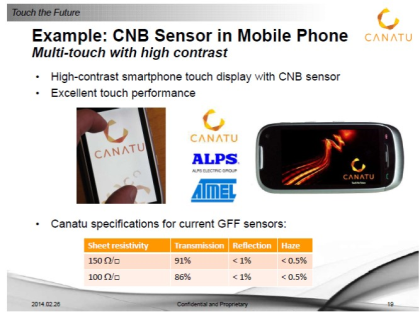
Progress at Canatu
David Brown presented Canatu's latest work. Canatu produces Carbon Nanotube films made from going straight from vapour phase to solid phase. The current specification for touch sensors are as follows:
Source: Canatu
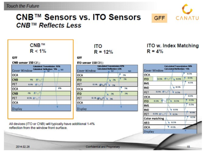
One of the benefits of Canatu's film is that the carbon nanotube layer has much better index matching to the display, compared to ITO, which needs multiple additional layers to improve the index match, as shown below.The company is also working on thin film transistors, having demonstrated transistors with a mobility of 35 cm2/Vs and on/off ratio of 6x10^6. For more information, subscribers can see our profile of Canatu at http://portal.idtechex.com/company-profiles/canatu-000064.asp.