What new electronic product is being researched by organizations in over 30 countries but none have sold anything yet? It is of huge significance to everyone in the electronic, printing, merchandising and healthcare industries, to name just a few. It is the printed transistor. To be more precise, it is Thin Film Transistor Circuits (TFTCs) that do not employ traditional crystalline or amorphous silicon, germanium or gallium arsenide and that can therefore be deposited at high speeds onto low cost flexible substrates.
Flexible transistor circuits using new compounds
Traditionally, semiconductors are made as crystalline as possible to optimise their performance but even that is no longer the case. The new transistors variously use thin films of organic or inorganic compounds as the semiconductors and gate dielectrics, enabling flexible transistor circuits. One printable inorganic semiconductor favoured by Toppan Printing and Tokyo Institute of Technology is an amorphous combination of InGaZnO, for example, and it can be cured at low temperature. Electrodes in the new transistors are sometimes metal but sometimes they consist of conductive organic compounds.
Similarities with old types of transistor
There are similarities with the old silicon chip and the amorphous silicon transistor array on the back of an LCD display today. The new transistors are Field Effect Transistors (FETs). Most use the forty year old geometry where the controlled current passes horizontally but some (e.g. ORFID Inc in the USA) use vertical geometry to reduce feature size, increase frequency and current carrying capacity and/or reduce cost. Almost all potential markets for these new transistors are for arrays of large numbers of transistors, not individual transistors. Putting p type and n type back to back in a Complementary Metal Oxide Semiconductor (CMOS) configuration is favoured with the new as with the old technology, for example, to save power. Although very high power versions for electrical use are also in prospect, they are not the largest potential market. Some of these circuits of hundreds to millions of transistors will involve other devices such as sensors, diodes and fuses deposited at the same time. All this is very similar to the old technologies. But there the similarities stop.
Remarkable capabilities
The new transistors can be deposited on low cost flexible substrates such as PET and PEN film, aluminium or stainless steel foil. As yet, they are much larger than today's silicon transistors but they can be one hundredth of the cost, thinner and lighter in weight. Every one can be made differently if required. In other words hard wired programming for a batch size of one is viable. Small runs and redesigns are still very low cost, in stark contrast to the situation with traditional transistors. Some are totally transparent. For example, proponent 3T Technologies in the UK calls itself the "Transparent electronics company". Some are much more stable than amorphous silicon, even working for years without protection from the elements. Some will be stretchable and even biodegradable and made on paper thanks to Abo Akademi and Helsinki University in Finland, ACREO and Linkoping University in Sweden and others.
Those new transistors that are printed, such as the Hewlett Packard ones using Zinc Oxide based transistors in thermal inkjet printers, can be made at very high speed, reel to reel over large areas. Such area is needed for driving the pixels of huge billboards and signage for example. Currently most of the new transistors are limited to frequencies around tens of megahertz, but this still embraces the most popular frequency for RFID permitting sales of trillions to be contemplated rather than the limit of no more than tens of billions yearly imposed by the cost of the silicon chip in today's RFID label.
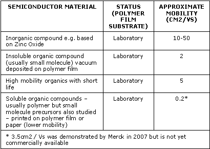
The higher the mobility of the charge carrier in the semiconductor, the higher the frequency of the transistor, all other things being the same. Improving printable and thin film semiconductors is therefore a hot area of research and some examples are given below, though the situation is rapidly changing.
Typical carrier mobility in different potential TFTC semiconductors (actual and envisaged)

Source IDTechEx report "Printed and Thin Film Transistors and Memory" www.IDTechEx.com/tftc
However, Plastic E Print in the UK has a version made in a single layer that can achieve terahertz frequency. Some printed transistors are fault tolerant and therefore of interest to NASA and the healthcare community. Eastman Kodak in the USA has recently patented edible printed RFID.
Huge new markets
The new transistors are the key to huge new markets that the silicon chip will never reach. They will transform medicine, for example, making sophisticated diagnostic and drug delivery skin patches viable and a multitude of disposable testers of bodily fluids. They will herald the smart package for merchandising, with moving colour images, sound and storage of books, videos etc as incentives. They will lead to safer dispensing of medicines, recording what was taken when, prompting and much, much more.
The largest segment of the total printed electronics industry (encompassing displays, sensors, photovoltaics etc) will be printed transistors and memory. They will drive lighting, displays, signage, electronic products, medical disposables, smart packaging, smart labels and much more besides. The chemical, plastics, printing, electronics and other industries are cooperating to make it happen. Already, over 150 organizations are developing printed transistors and memory, with first products being used in 2007. The market will take off slowly initially, reaching $40 Million in 2009 then grow rapidly as technical challenges are overcome, reaching $8 Billion by 2017.
Comprehensive new report
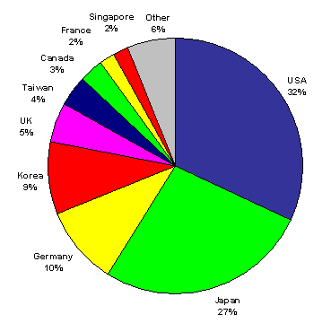
IDTechEx has a new report "Printed and Thin Film Transistors and Memory". It explains the many chemical and construction technologies of the new transistors and memory, profiles a large number of the developers and their plans, and forecasts the market size for 2007 to 2017, as the first production products burst on the scene and a multi-billion dollar business is created. 150 organizations developing the new transistors are compared. They are distributed as follows.
Distribution of 150 organizations developing printed transistors

Source IDTechEx report "Printed and Thin Film Transistors and Memory" www.IDTechEx.com/tftc
The report gives the big picture - organic and printed inorganic thin film transistor circuits with coverage of company progress from around the World. All those involved or seeking to get involved in this topic must read this report or risk getting left behind.
These transistors are the engine of the emerging printed and potentially printed electronics market. That will become a $300 billion business and many billion dollar companies will be created on the back of it, transforming many sectors of society and industry. No one can ignore that. To learn more see www.IDTechEx.com/tftc.
Top image: PolyIC


